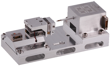
PI 85 SEM PicoIndenter Nanomechanical Test Instrument
The PI 85 SEM PicoIndenter is a depth-sensing indenter that can be interfaced with a scanning electron microscope (SEM). With this system it is possible to perform quantitative nanomechanical testing while simultaneously imaging with the scanning electron microscope. Coupling these two techniques allows the researcher to position the probe with extreme accuracy and to image the deformation process throughout the test.
This system is designed for exceptional performance in the electron microscope, with a vacuum-compatible transducer and a conductive boron-doped diamond probe. With Hysitron's 3-plate capacitive transducer, force is applied electrostatically and displacement is measured capacitively. This low-current design provides low thermal drift and industry-leading stability and sensitivity.
The PI 85 system is ideal for characterizing fracture onset and crack propagation, delamination, and pile-up. Also, time-sensitive phenomena such as viscoelastic behavior can be observed in real time rather than "post mortem." The pairing of these two high-resolution techniques provides unique insight into the mechanisms responsible for materials behavior.
|
PI 85 SEM PicoIndenter
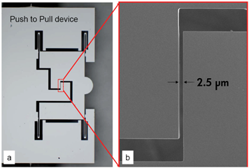
Push to Pull device |
Transducer Specifications:
- 30 mN maximum load
- ≤ 3 nN Load Resolution
- ≤ 400 nN RMS Force Noise Floor
- ≤ 0.02 nm Displacement Resolution
- ≤ 1 nm RMS Displacement Noise
Option Assemblies of PI 85 PicoIndenter
• Push to Pull (PTP) –
Hysitron has developed the Push-to-Pull (PTP) device*, an in-situ tensile apparatus designed to work seamlessly with Hysitron’s commercially available PI Series PicoIndenter for TEM and SEM.
This PTP apparatus not only enables quantitative tensile load-displacement data simultaneously with real time images of the microstructure behavior, it also simplifies the sample preparation procedure, and serves as an energy buffer, strain sensor, and force calibration.
The PTP device is a consumable, though multi-use MEMS-fabricated apparatus. The portability of the device allows for easy transfer between FIB and SEM/TEM.
|