Silicon-based transistors have led the world in following the Moore's law in the past few decades. To keep the Moore's law, the two-dimensional (2D) semiconductor is highly anticipated to be one of the possible solutions. One of the families of these 2D semiconductors is Transition metal dichalcogenide (TMD). The high mobility and atomic thickness of TMD materials are both crucial properties that keep the size of the transistor scaling. With the collaboration with TSMC, our Lab research focuses on solving obstacles for fabricating high-performance 2D electronics, including reducing the contact resistance of 2D electronics and developing the doping technique for 2D materials.
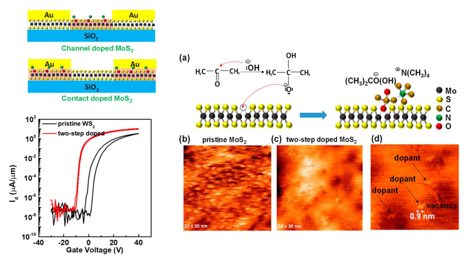
Here, we developed a two-step doping method for effectively doping 2D materials through a defect repairing process. The method achieves strong and hysteresis-free doping and is suitable for use with the most widely used transition-metal dichalcogenides. Through our method, we achieved a record-high sheet conductance (0.16 mS·sq-1 without gating) of monolayer MoS2 and a high mobility and carrier concentration (4.1 × 1013 cm-2). (ACS Nano, 17, 2653, (2023))
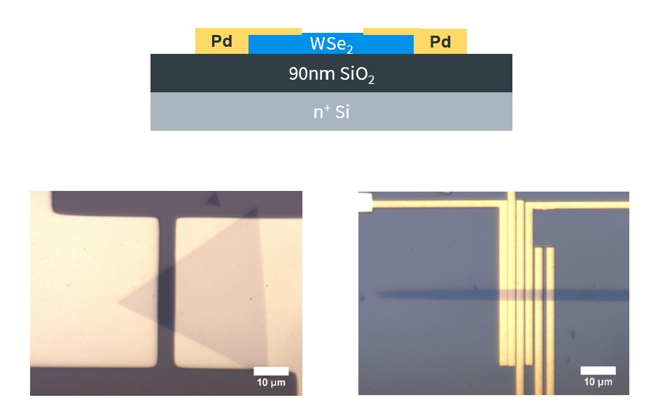
Further, we also focus on the development of high-performance p-type 2D transistors, which are crucial in 2D electronics. We’re now developing the p-type doping technique which concept is based on our previous work (ACS Nano, 17, 2653, (2023)). We start from fabricate the WSe2 microscale device to confirm the doping effect and other dopant properties testing. We also able to access the Helium Ion Beam Microscope (HIBM) to fabricate the nanometer device. We expect to develop the p-type doping technique applying on 2D device for the high performance p-type transistor.