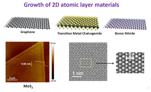
We have been focusing on developing two-dimensional (2D) atomic layer materials such as graphene, transition metal dichalcogenide (TMD), or other new 2D materials on optics, electronics, and optoelectronics. We are also dedicated to the growth of high-quality 2D materials. In addition to exploring the fundamental science of 2D materials, we are also interested in the development of industrial applications of 2D materials with company such as TSMC. The following are a few examples of our research results on 2D materials.
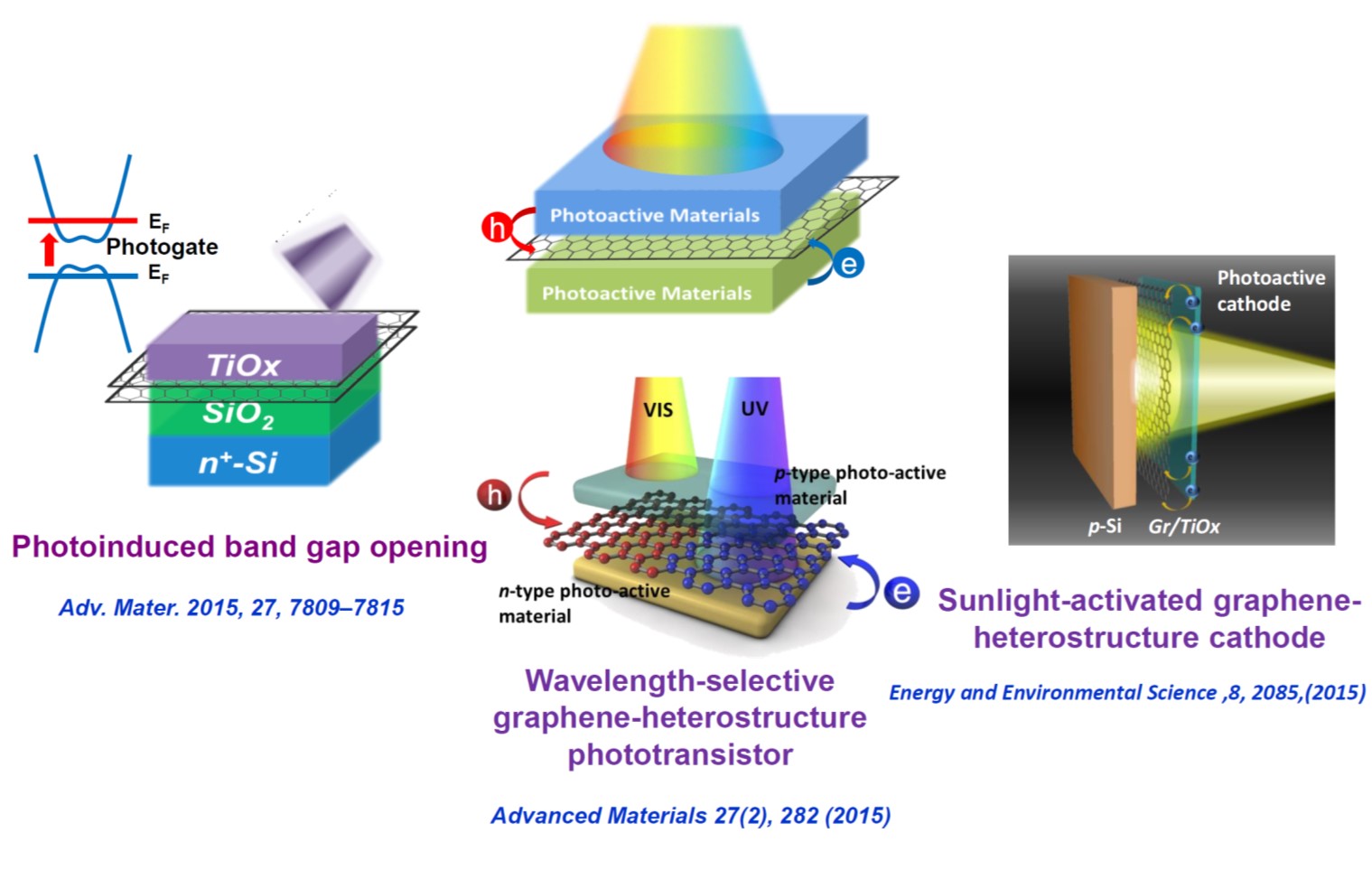
These works represent strong light-matter interactions at graphene-heterostructures, which can be applied to several interesting devices such as photovoltaics or photodetectors. For example, a novel “sunlight-activated graphene-heterostructure transparent electrode was developed (Energy and Environmental Science, 8, 2085 (2015)). Photogenerated charges from alight-absorbing material are transferred to graphene, resulting in the modulation of electrical properties of the graphene transparent electrode caused by a strong light–matter interaction at graphene-heterostructure interfaces. Another example is demonstrating remarkably strong photoinduced doping at a graphene/titanium oxide (TiOx) heterostructure. The trap-state mediated photoinduced charge transfer from the remote bulk TiOx ultrathin film to graphene, similar to photoinduced modulation doping, resulted in a strikingly high n-type doping level of greater than ≈ 10 13 cm -2 , which is much higher than that of any other reported photoinduced doping techniques. (Advanced Materials, 27, 7809, 2015).
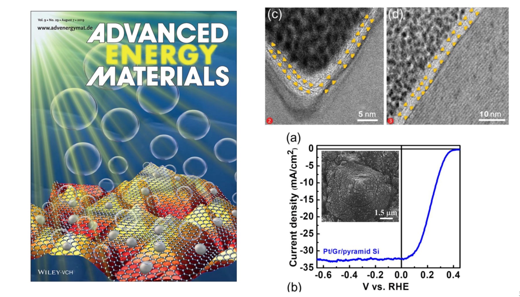
This work presents a novel photo-electrochemical architecture based on the 3D pyramid-like graphene/p-Si Schottky junctions. The formation of 3D pyramid-like graphene/p-Si Schottky junctions exhibits enhanced electrochemical activity and promotes charge separation efficiency. The inherent chemical inertness of graphene significantly improves the operational stability of 3D graphene/p-Si Schottky junction photo-electrochemical cells. The 3D pyramid-like graphene/p-Si Schottky junction photocathode delivers an onset potential of 0.41 V and a saturated photocurrent density of −32.5 mA cm-2 at 0 V (vs RHE) with excellent stability comparable to values reported for textured or nanostructured p-Si photocathodes coated with ultrathin oxide layers by the conventional atomic layer deposition technique. (Advanced Energy Materials, 1901022, (2019))
Based on this simple and clean transfer method, we may also use a commercially available screen protector of a smart phone with electrostatic adherence to transfer an organic-residue-free graphene film. (See the corresponding video file) The CLT technique which does not involve using any organic support or adhesives can produce residual-free and high-quality graphene films for large-area processability, and has great potential for future industrial production of flexible graphene-based electronics or optoelectronics. (Advanced Materials, 25, 4521, (2013))
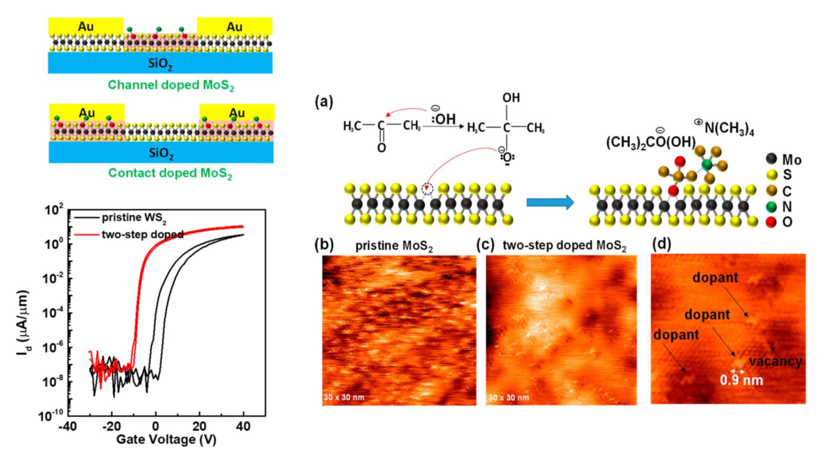
Here, we developed a two-step doping method for effectively doping 2D materials through a defect repairing process. The method achieves strong and hysteresis free doping and is suitable for use with the most widely used transition-metal dichalcogenides. Through our method, we achieved a record-high sheet conductance (0.16 mS·sq-1 without gating) of monolayer MoS2 and a high mobility and carrier concentration (4.1 × 1013 cm-2).(ACS Nano, 17, 2653, (2023))
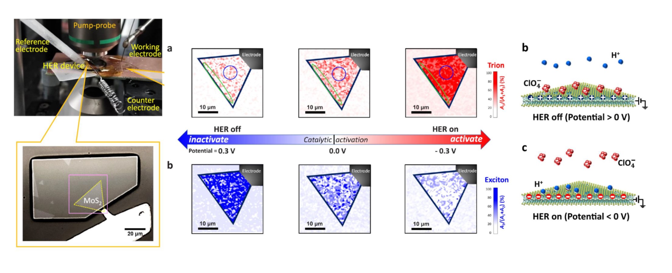
Using the distinct carrier relaxation dynamics of excitons and trions of monolayer MoS2 as sensitive descriptors, an in situ microcell based scanning time-resolved liquid cell microscope is set up to simultaneously measure the bias-dependent exciton/trion dynamics and spatially map the catalytic activity of monolayer MoS2 during the HER. This operando probing technique used to monitor the interplay between exciton/trion dynamics and electrocatalytic activity for two-dimensional transition metal dichalcogenides provides an excellent platform to investigate the local carrier behaviors at the atomic layer/liquid electrolyte interfaces during electrocatalytic reaction.(ACS Nano, 16, 4298, (2022))