Research Profile – Chia-Hao Lee
Department of Materials Science and Engineering, National Taiwan University
|
Chia-Hao LeeM.S. in Materials Science and Engineering, NTU, 2016
B.S.E. in Materials Science and Engineering, NTU, 2014
|
 |
 |
|
Expertises Ultra-High Vacuum Techniques, TEM analysis, and Growth of Nanomaterials |
|||
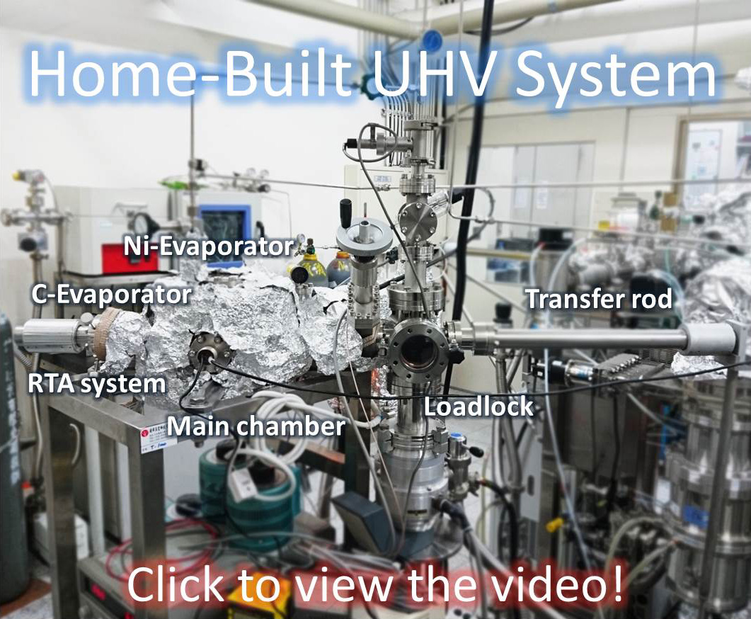
I designed and built this Ultra-High Vacuum CVD system from scratch to fabricate nickel silicides (Ni2Si, NiSi, NiSi2) on Si substrates without surface oxidation for graphene growth. I've also employed as a TEM teaching assistant for 2 years by the Department of Materials Science and Engineering at NTU. |
|||

Research Projects |
|
| High-Quality Graphene Growth on Nickel Silicide Substrates by UHVCVD | |
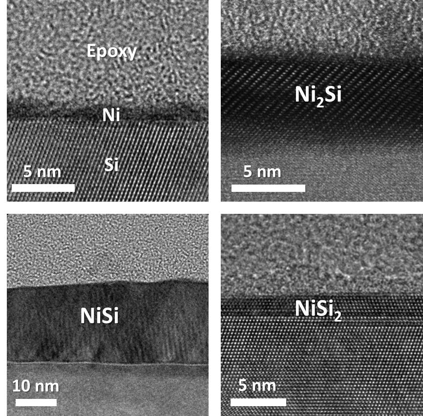
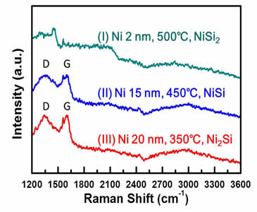
Graphene has been in the focus of intensive researches due to its unique physical properties. For almost ten years, the synthesis of large-area high-quality graphene has been an important but unsolved problem. The routine method for graphene growth is the CVD process with Cu substrates. However, it requires high growth temperature (1000℃) and complicated transferring process to fabricate grahene-based devices. Therefore, to further integrate graphene into Si-based energy-saving transistors, we proposed to directly synthesize graphene on nickel silicides (Ni2Si, NiSi, and NiSi2), which are the common contact materials in VLSI technology. To avoid surface oxidation of silicides, I spent one year to build an unique Ultra-High Vacuum Chemical Vapor Deposition (UHVCVD) system. It is equipped with two home-made evaporators (Ni, C), a rate monitor, rapid thermal annealing system, and a specialized sample holder, which is a delicate design. I examined the catalytic ability of three nickel silicides, and our results show that Ni2Si exhibits the highest catalytic ability over other nickel silicide substrates, paving the way for direct growth of graphene on contact materials. The manuscript regarding these results are in preparation for submission. |
|
 |
|
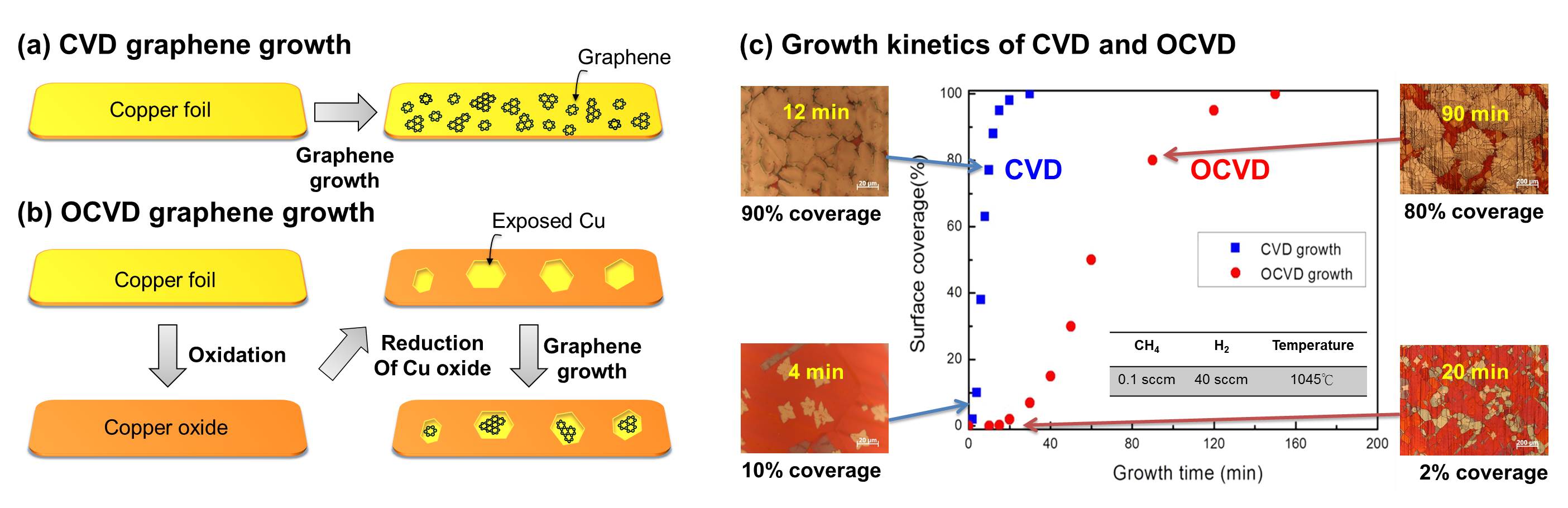
| Large-Domain Graphene Growth on Cu by Oxygen-Assisted CVD | |
Catalytic growth of graphene on Cu substrates via the CVD process is the most promising and economic method to enable industrial-scale production of graphene. However, high-density domain boundaries are present in the CVD graphene. These domain boundaries degrade the carrier transport properties and mechanical strength of graphene sheets. We established an oxide-assisted chemical vapor deposition method (denoted as OCVD), which can largely decrease its defect density by forming an oxide passivation layer before the nucleation stage of graphene. With the significant reduction of nucleation density of graphene (From 104 to 1 mm-2), the transport properties of graphene-based device have been largely improved (Hole mobility: 3270 cm2/V·s). The paper regarding the results has been published by Nanoscale.
R. J. Chang, C. H. Lee, M. K. Lee et al., “Effects of Surface Oxidation of Cu substrates on the Growth Kinetics of Graphene by Chemical Vapor Deposition”, Nanoscale, 2017, DOI: 10.1039/C6NR09341H
|
|
|
|