|
Nanoimprint & Nanofabrication |
|||||
Laser Annealing
Nanopaticle Stacks
(INC) method
Silicon Solar Cells & Antireflection Coating Nanoparticles Nanoimprint & Nanofabrication Organic Solar Cells Carbon Nanotube |
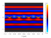
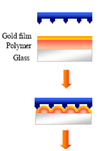
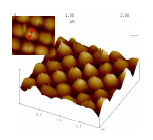
Nano-imprinting in metal (NIM) We describe a thermal embossing imprint method, which we name “nano-imprinting in metal” (NIM), for patterning metal films with a variety of profiles. Metal films exhibiting either perforated hole-arrays or corrugated structures with various surface morphologies can be fabricated rapidly. The SPR phenomenon allowed energy coupling to the other side of the textured metal film, causing a dramatic increase in the transmission. As a technique for readily controlling the working wavelength and transmittance, the NIM method has great potential for application in various optoelectronic devices. |
|
|||
Copyright(c) 2008 Nano-optpelectronics Lab., Department of Material Science and Engineering, National Taiwan University No. 1, Sec. 4, Roosevelt Road, Taipei, 10617 Taiwan(R.O.C) Phone:+886-2-3366-3240 Fax:+886-2-2362-7651 |
|||||