
|
|||
本研究開發之矽基材上之深溝槽狀薄層金屬結構,可用以偵測通訊波段紅外光  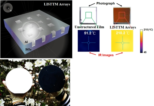
奈米金屬團簇用於光收成及場發射元件的研究被Energy
& Environmental Science期刊選為當期之封面
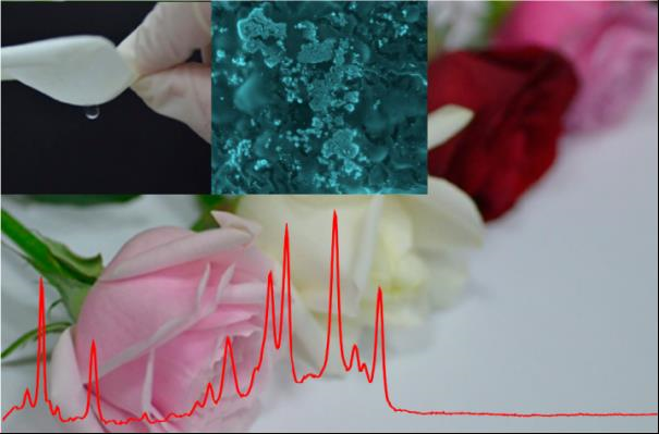 
(左)超疏水濃縮效應,於玫瑰花花瓣上濃縮聚集銀奈米粒子。
(左)奈米感測器研究被選為期刊封面。 (右)表面電漿成功地擷取原本損失於金屬電極上之大量能源,發表於Energy & Environmental Science
 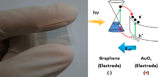 (左) 有關奈米碳管光學性質之研究被選為Nature Asia Material Highlight (右)石墨烯/氧化金光偵測器可適用於 picowatt 強度的弱光偵測發表於ACS Nano
  利用漸變折射率奈米粒子大幅增加(a)太陽能電池廣角度光收成效率(b)固態照明元件光取出效率的研究刊登於Advanced Functional Materials期刊,同時被Nanowerk Spotlight網站置於首頁報導:Stacked nanoparticle layers shine new light on optical thin films |
|||
|
1. P. C. Hsieh, S. W. Chang, W. H. Kung, T. C. Hsiao, and H. L. Chen*, “Epsilon-near-zero thin films in a dual-functional system for thermal infrared camouflage and thermal management within the atmospheric window,” Materials Horizons, accepted, (2024) (highlighted on the Journal Back Cover). 2.
P. H. Lan, C. W. Hwang, T. C. Chen, T. W. Wang, H. L. Chen* ,and Dehui Wan*
“Hierarchical Ceramic Nanofibrous Aerogels for Universal Passive Radiative Cooling,” Advanced Functional Materials,
(2024), 2410285.
3.
Q. T. Le, S. W. Chang, B. Y. Chen, H. A. Phan, A. C. Yang, F. H. Ko, H. C. Wang, N. Y. Chen*,
H. L. Chen*
, Dehui Wan*
“AI-enabled design of extraordinary daytime radiative cooling materials,” Solar Energy Materials and Solar Cells, 278
(2024), 113177..
4.
C. M. Kan, S. W. Chang, J. Y. Li, J. C. Cisneros, and
H. L. Chen*,
“Optically manipulated nitrate-salt-based direct absorption solar collectors for a photothermal energy harvesting system,”
Chemical Engineering Journal, Vol. 498, 15 October, (2024), 155317.
5.
S. W. Chang, Y. J. Chen, Dehui Wan, and
H. L. Chen*,
“Black and white: a bifunctional optical standard for near-perfect white light diffuse reflection and blackbody radiation,”
Optica, Vol. 11, Issue 9, (2024) pp. 1303-1312.
6.
S. H. Chen, S. W. Chang, and
H. L. Chen*,
Characterization of 2D Transition Metal Dichalcogenides Through Anisotropic Exciton Behaviors,”
Small Method,, Vol. 8, No. 5 (2024), 2301061 (highlighted on the Journal Back Cover).
7.
Y. J. Chen, S. W. Chang, H. C. Wang, S. K. Lim, C. I. Huang, F. H. Ko, Y. C. Lo, Dehui Wan*, and
H. L. Chen*,
“ Daytime radiative cooling of single-board computer in nearly enclosed unmanned surface vehicle,”
Solar Energy Materials and Solar Cells, 268 (2024), 112723. 8.
C. C. Lai, T. C. Hsiao, W. H. Wang, S. W. Chang, and
H. L. Chen*,
“Emissivity and Optical Properties of Thin-film Metallic Glass in the
Thermal Infrared Region,”
Advanced Optical Materials, (2023) accepted (highlighted on the Journal Inside Front Cover). 9.
S. W. Chang, Y.
J. Chen, Dehui Wan, H. L. Chen* “Near-Room-Temperature Waste
Heat Recovery Through Radiative Cooling for Both Daytime and Nighttime
Power Generation”, Journal of
Materials Chemistry A, (2023), 11, 15183-15195 (highlighted on the
Journal Back Cover). 10.
S. H. Tsao, A. Y. Sun, Y. C.
Lee, C.-W. Hwang, K.-T. Lin, Y. S. Lai, L. C. Yang, H. L. Chen*,
Dehui Wan* “Solution-Processable Three-Dimensional Metamaterials with
Ultrahigh Broadband Absorption for Photothermal Electronic
Conversion”, Laser & Photonics Reviews, (2023), 17, 2300315. 11.
Y. H. Chen, C. C. Chen, L. C.
Lu, C. Y. Lan, H. L. Chen*, T.-H. Yen*, Dehui Wan* “Wafer-scale
Fibrous SERS Substrates Allow Label-Free, Portable Detection of Food
Adulteration and Diagnosis of Pesticide Poisoning”,
Sensors and Actuators B:
Chemical, (2023), 391,
134035. 12.
Y. H. Chen, C.
W. Hwang, S. W. Chang, M. T. Tsai, K. N. Jayakumaran, L. C. Yang, Y.
C. Lo, F. H. Ko, H. C. Wang, H. L. Chen,* Dehui Wan*
“Eco-Friendly Transparent Silk Fibroin Radiative Cooling Film for
Thermal Management of Optoelectronics”,
Advanced Functional Materials,
(2023), 33, 2301924 (highlighted on the Journal Inside Back Cover). 13.
H. Y. Lin, W. R. Chen, L. C.
Lu, H. L. Chen, Y. H. Chen, M. Pan, C. C. Chen, C. Chen*, T. H.
Yen*, Dehui Wan* “Direct Thermal Growth of Gold Nanopearls on 3D
Interweaved Hydrophobic Fibers as Ultrasensitive Portable SERS
Substrates for Clinical Applications”,
Small, (2023), 19, 2207404
(highlighted on the Journal Frontispiece). 14.
M. T. Tsai, S. W. Chang, Y. J.
Chen, H. L. Chen, P. H. Lan, D. C. Chen, F. H. Ko, Y. C. Lo, H.
C. Wang, Dehui Wan* “Scalable, Flame-resistant, Superhydrophobic
Ceramic Metafibers for Sustainable All-day Radiative Cooling”,
Nano Today, (2023), 48,
101745. 15.
Y. C. Lee, S.
W. Chang, S. H. Chen, S. L. Chen,
and
H. L. Chen*, “Optical inspection of two-dimensional materials: From mechanical
exfoliation to wafer-scale growth and beyond,”
Advanced Science, (2022), 9, 2102128 16.
Y. L. Chang, I.
C. Lai, L. C. Lu, S. W. Chang, A. Y. Sun, D. Wan*,
and H. L. Chen*
“Wafer-scale nanocracks enable single-molecule detection and on-site
analysis,” Biosensors and
Bioelectronics, 200, (2022) 113920 17.
Y. C. Tseng, S. W. Chang, Y. C. Lee, and
H. L. Chen*,
“Cavity-enhanced magnetic dipole resonance induced hot luminescence
from hundred-nanometer-sized silicon spheres,”
Nanophotonics, (2022)
11(16): 3583–3593 18.
S. L. Chen, S. W Chang, Y. J. Chen, and H. L. Chen*, “Possible
warming effect of fine particulate matter in the atmosphere,”
Communications Earth and
Environment, 2, 208 (2021) 19.
C. C. Lin,
B. J. Chang,
S. H. Chen, K. T. Lin,
S. W.
Chang,
W. Y.
Chen,
B. Y Chen, M. C.
Liu, and
H. L. Chen*, “Gallium arsenide–based active antennas for optical communication
photodetection with robustness to voltage and temperature,”
Advanced Optical Materials,
9, 2100165
(1-12) (2021) DOI: 10.1002/adom.202100165 20.
S. L. Chen, C. C. Yu, S. W. Chang, Y. C. Lee, and H. L. Chen*,
“Optimization and simulation of a carbon nanotube arrangement for
transparent conductive electrodes with record-high direct current to
optical conductive ratios,”
Optical Materials Express, Vol. 11, No. 4 / 1205-1217 (2021) 21.
A. Y. Sun, Y. C. Lee, S. W. Chang, S. L. Chen, H. C. Wang, Dehui Wan*, and
H. L. Chen, “Diverse Substrate-Mediated Local Electric Field
Enhancement of Metal Nanoparticles for Nanogap Enhanced Raman
Scattering,” Analytical
Chemistry, 93, 4299-4307 (2021) 22.
T. Y Lin, K. T. Lin, C. C. Lin, Y. W. Lee, L. T. Shiu, W. Y. Chen and H.
L. Chen*, “Magnetic fields affect hot electrons in silicon-based
photodetectors at telecommunication wavelengths,”
Materials Horizons, 6, 1156-1168
(2019) (Inside
Back Cover期刊封面) 23.
S. J. Kuo, S. W. Chang, Y. Y. Hui, O. Y. Chen, Y. W Chen, C. C. Lin, Dehui
Wan, H. L. Chen*, and H. C. Chang*, “Fluorescent Microdiamonds Conjugated with Hollow Gold
Nanoparticles as Photothermal Fiducial Markers in Tissue,”
Journal of Materials Chemistry C, 7, 15197-15207 (2019) 24.
K.
T. Lin, C.
J. Chan, Y.
S. Lai*, L.
T. Shiu, and
H. L. Chen*, “Silicon-Based
Embedded Trenches of Active Antennas for High-Responsivity
Omnidirectional Photodetection at Telecommunication Wavelengths”,
ACS
Applied Materials & Interfaces, Volume 11, Issue 3, 3150–3159, (2019)
(Supplementary Cover期刊封面) 25.
C-K Ku, P-H Wu, C-C Chung, C -C Chen, K-J Tsai, H-M Chen, Y-C Chang, C-H
Chuang, C-Y Wei, C-Y Wen, T-Y Lin, H. L. Chen, Z-Y Lee, J-R
Chang, Y-S Wang, D-Y Wang, Bing Joe Hwang, Chun-Wei Chen, “Creation of
three-dimensional textured graphene/Si Schottky junction photocathode
for enhanced photoelectrochemical efficiency and stability”,
Advanced Energy Materials,
1901022, (2019) (Back
Cover期刊封面) 26.
T. Y. Lin, Y. C. Lee, Y. W. Lee, S. W. Chang, D. L. Ma, B. C. Lin, H. L.
Chen*, “Air Gap-Based Cavities Dramatically Enhance the True
Intrinsic Spectral Signals of Suspended and Pristine Two-Dimensional
Materials,” The Journal of
Physical Chemistry C,
123 (9), 5667-5679 (2019) 27.
Y. C. Tseng, T. Y Lin, Y. C. Lee, C. K. Ku, C. W Chen, and H. L. Chen*,
“Magnetic dipole resonance and coupling effects directly enhance the
Raman signals of as-grown graphene on copper foil by over a
hundredfold,” Chemistry of
Materials, 30, 1472-1483 (2018) 28.
S. J. Kuo, P. C. Tsai, Y. C. Lee, S.
W. Chang, S. Sotoma, C. Y. Fang, H. C. Chang and H. L. Chen*,
“Manipulating the distribution of electric field intensity to
effectively enhance the spatial and spectral fluorescence intensity of
fluorescent nanodiamonds,”
Nanoscale, Vol. 10 No. 37 pp. 17576–17584 (2018)
(當期期刊內封面) 29.
K. T. Lin, H. L. Chen*, Y. S. Lai,* C. C. Yu, Y. C. Lee, P. Y. Su,
Y. T. Yen, and B. Y. Chen, “Loading effect–induced broadband perfect
absorber based on single-layer structured metal film,”
Nano Energy, 37, 61–73 (2017) 30.
Y. C. Lee, Y. C. Tseng, and H. L. Chen*, “Single Type of Nanocavity
Structure Enhances Light Outcouplings from Various Two-Dimensional
Materials by over 100-Fold,” ACS
Photonics 4, 93−105 (2017) 31.
Y. C Tseng, Y. C. Lee, S. W. Chang, T. Y. Lin, D. L. Ma, B. C. Lin, and
H. L. Chen*, “Enhancing Raman Signals through Electromagnetic Hot
Zones Induced by Magnetic Dipole Resonance of Metal-Free
Nanoparticles,” Nanotechnology,
28 (2017) 465202. 32.
C. C. Yu, K. T. Lin, P. Y. Su, E. Y. Wang, Y. T. Yen, and H. L. Chen*,
“Short-Range Plasmonic Nanofocusing Within Submicron Regimes
Facilitates In Situ Probing and Promoting of Interfacial Reactions,”
Nanoscale, (2016) 8, 3647–3659. 33.
Y. C. Lee, K. T. Lin, H. L. Chen*, “Ultra-broadband and
omnidirectional enhanced absorption of graphene in a simple nanocavity
structure,” Carbon, 108
(2016) 253-261. (SCI) 34.
Y. C. Tseng, Y. C. Cheng, Y. C. Lee, D. L. Ma, B. Y. Yu, B. C. Lin, and
H. L. Chen*, “Using Visible Laser-Based Raman Spectroscopy to
Identify the Surface Polarity of Silicon Carbide,”
Journal of Physical Chemistry C,
(2016), 120, 18228−18234. (SCI) 35.
K. T. Lin, H. L. Chen*, Y. S. Lai*, “Filter-free, junctionless
structures for color sensing,”
Nanoscale, 8, 16936–16946 (2016) (SCI) 36.
K. T. Lin, H. L. Chen*, Y. S. Lai,* Y. M Chi, and T. W. Chu,
“Plasmonics-Based Multifunctional Electrodes for Low-Power Consumption
Compact Color-Image Sensors,”
ACS Applied Materials & Interfaces, 8, 6718−6726 (2016) (SCI) 37.
T. Y. Lu, Y. C. Lee, Y. T. Yen, C. C. Yu, and H. L. Chen*,
“Astronomical liquid mirrors as highly ultrasensitive, broadband
operational surface-enhanced Raman scattering-active substrates,”
Journal of Colloid and Interface
Science, (2016) Volume 466, 15 March, Pages 80-90 (SCI) 38.
Y. L. Liu, C. C. Yu, K. T. Lin, T. C. Yang, E. Y. Wang, H. L. Chen*,
L. C. Chen, and K. H. Chen, “Transparent, Broadband, Flexible, and
Bifacial-Operable Photodetectors Containing a Large-Area Graphene-Gold
Oxide Heterojunction,” ACS Nano
Vol. 9, No. 5, 5093–5103 (2015). 39.
S. H. Tsao, Dehui Wan, Y. S. Lai, H. M. Chang, C. C. Yu, K. T. Lin, and
H. L. Chen, “White Light–Induced Collective Heating of Gold
Nanocomposite/B. mori Silk Thin Films with Ultrahigh Broadband
Absorbance,” ACS Nano accepted DOI: 10.1021/acsnano.5b04913 (2015) 40.
Y. C. Lee, H. L. Chen*, C. Y.
Lu, H. S. Wu, Y. F. Chou and S. H. Chen, “Using nanoimprint
lithography to improve the light extraction efficiency and color
rendering of dichromatic white light-emitting diodes,“
Nanoscale, (2015)
7, 16312-16320 (SCI) 41.
S. Y. Chou, C. C. Yu, Y. T Yen, K. T. Lin, H. L. Chen*, and W. F.
Su, “Romantic Story or Raman
Scattering? Rose Petals as Eco-friendly, Low-Cost Substrates for
Ultrasensitive Surface-Enhanced Raman Scattering,”
Analytical Chemistry, 87,
6017−6024 (2015) (SCI) 42.
C. C. Yu, S. Y. Chou, Y. C. Tseng, S. C. Tseng, Y. T. Yen and H. L.
Chen*, “Single-shot laser treatment provides quasi-three
dimensional paper-based substrates for SERS with attomolar
sensitivity,” Nanoscale, 7,
1667–1677 (2015) (SCI)
(當期期刊封面) 43.
Y. C. Lee, E. Y. Wang, Y. L. Liu, and H. L. Chen*, “Using Metal-less
Structures To Enhance the Raman Signals of Graphene by 100-fold while
Maintaining the Band-to-Band Ratio and Peak Positions Precisely,”
Chemistry of Materials, 27,
876−884 (2015) (SCI) 44.
P. H. Ho, W. C. Lee, Y. T. Liou, Y. P. Chiu, Y. S. Shih, C. C. Chen, P. Y.
Su, M. K. Li, H. L. Chen, C. T. Liang, C. W. Chen*,
“Sunlight-activated graphene-heterostructure transparent cathodes:
enabling high-performance n-graphene/p-Si Schottky junction
photovoltaics,” Energy & Environmental Science, 8, 2085--2092 (2015) (SCI) 45.
C. C. Yu, Y. C. Tseng, P. Y. Su, K. T. Lin, C. C. Shao, S. Y. Chou, Y. T.
Yen, H. L. Chen*, “Incident Angle–Tuned, Broadband,
Ultrahigh-Sensitivity Plasmonic Antennas Prepared from Nanoparticles
on Imprinted Mirrors,” Nanoscale,
7, 3985–3996 (2015) (SCI) (當期期刊內封面)(2015 Hot Papers in Nanoscale) 46.
C. C. Yu, H. L. Chen*, “Nanoimprint technology for patterning
functional materials and its applications,”
Microelectronic Engineering,
132, 98-119 (2015) (SCI) (30 year
Anniversary Special Issue, Invited Review article) 47.
K. T. Lin, H. L. Chen*, Y. S. Lai,* and C. C. Yu, “Silicon–based
broadband antenna for high–responsivity and polarization–insensitive
photodetection at telecommunication wavelengths,”
Nature Communications, 5,
3288, DOI: 10.1038/ncomms4288 (2014) (SCI) 48.
Y. L. Liu, C. C. Yu, K. T. Lin, E. Y. Wang, T. C. Yang, H. L. Chen*,
C. W. Chen, C. K. Chang, L. C. Chen, and K. H. Chen, “Nondestructive
Characterization of the Structural Quality and Thickness of Large-Area
Graphene on Various Substrates,”
Analytical Chemistry 86, 7192-7199 (2014) (SCI)
(Editors’
Highlight)
49.
Y. L. Liu, C. Y. Fang, C. C. Yu, T. C. Yang, and H. L. Chen*,
“Controllable localized surface plasmonic resonance phenomena in
reduced gold oxide films,”
Chemistry of Materials, 26, 1799−1806 (2014) (SCI) 50.
K. T. Lin, H. L. Chen*, Y S. Lai*, Y. L. Liu, Y. C. Tseng, and C. H.
Lin, “Nanocrystallized CdS beneath the Surface of a Photoconductor for
Detection of UV Light with Picowatt Sensitivity,”
ACS
Applied Materials & Interfaces, 6,
19866−19875
(2014) (SCI) 51.
C. C. Yu, K. T. Lin, Y. C. Tseng, S. Y. Chou, C. C. Shao, H. L. Chen*
and W. F. Su, “Plasmonic nanoparticle-film calipers for rapid and
ultrasensitive dimensional and refractometric detection,”
Analyst, 139, 5103-5111 (2014) (SCI) 52.
Y. T. Yen, T. Y. Lu, Y. C. Lee, C. C. Yu, Y. C. Tsai, Y. C. Tseng, and
H. L. Chen*, “Highly reflective liquid
mirrors: Exploring the effects of localized surface plasmon resonance
and the arrangement of nanoparticles on metal liquid-like films,”
ACS Applied Materials & Interfaces, 6, 4292−4300
(2014) (SCI) 53. Y. C. Chen, P. Y. Su, S. C. Tseng, Y. C. Lee, and H. L. Chen*, “Preparing wafer-scale omnidirectional broadband light-harvesting nanostructures in a few seconds,” Journal of Materials Chemistry A, 2, 4633–4641 (2014) (SCI) 54.
Y. L. Liu, C. C. Yu, C. Y. Fang, H. L. Chen*, C. W. Chen, C. C. Kuo,
C. K. Chang, L. C. Chen, and K. H. Chen, “Using optical anisotropy as
a quality factor to rapidly characterize structural qualities of
large-area graphene films,”
Analytical Chemistry 85, 1605−1614 (2013) (SCI) 55.
K. T. Lin, S. C. Tseng, H. L. Chen*, Y. S. Lai,* S. H. Chen, Y. C.
Tseng, T. W. Chu, M. Y. Lin and Yen-Pei Lu, “Ultrahigh-sensitivity CdS
photoconductor with instant response and ultralow power consumption
for detection in low-light environments,”
Journal of Materials Chemistry C,
(2013)
Vol. 1, No. 27,
4244–4251 (SCI)
(當期期刊封面) 56.
C. Y. Fang, Y. L. Liu, Y. C. Lee, H. L. Chen*, D. H. Wan, and C. C.
Yu, “Nanoparticle Stacks with Graded Refractive Indices Enhance the
Omnidirectional Light Harvesting of Solar Cells and the Light
Extraction of Light-Emitting Diodes,”
Advanced Functional Materials,
(2013) 23, 1412–1421 (SCI)
(Nanowerk網站首頁報導) 57.
S. C. Tseng, C. C. Yu, D. C. Lin, Y. C. Tseng, H. L. Chen*, Y. C.
Chen, S. Y. Chou, and L. A. Wang, “Laser-induced jets of
nanoparticles: Exploiting air drag forces to select the particle size
of nanoparticle arrays,”
Nanoscale, 5, 2421–2428 (2013) (SCI) 58.
Y .C. Lee, T. Y. Lu, Y. H. Lai, H. L. Chen*, D. L. Ma*, C. C. Lee
and S. C. Cheng, “Simulations of light extraction and light
propagation properties of light emitting diodes featuring silicon
carbide substrates,” Optical
Materials (2013) 35, 1236-1242 (SCI) 59.
Yu Wang, S. S. Li, Y. C. Yeh, C. C. Yu, H. L. Chen, F. C. Li, Y. M.
Chang and Chun-Wei Chen, “Interactions between fluorescence of
atomically layered graphene oxide and metallic nanoparticles,”
Nanoscale, 5, 1687–1691 (2013) (SCI) 60.
Y. M. Chi, H. L. Chen*, Y S. Lai*, H. M. Chang, Y. C. Liao, C. C.
Cheng, S. H. Chen, S. C. Tseng, and K. T. Lin, “Optimizing Surface
Plasmon Resonance Effects on Finger Electrodes to Enhance the
Efficiency of Silicon-Based Solar Cells,”
Energy & Environmental Science
6, 935–942
(2013)
(SCI) 61.
Srikanth Ravipati, Jiann Shieh, F. H. Ko, C. C. Yu and H. L. Chen,
“Ultralow reflection from a-Si nanograss/Si nanofrustum double
layers,” Advanced Materials,
25, 1724–1728 (2013) (SCI) 62.
M. Y. Lin, Y. P. Lu, Y. S. Yang, H. L. Chen, C. H. Yang, A. M.
Grumezescu, E. C. Wang, Y. S. Lai, “Alignment of Stretchable
Nanoparticle Chains with Tunable Optical Properties Formed from
Molecular Machinery,” Current
Organic Chemistry, Volume 17, Number 2, January, 144-148(5) (2013)
(SCI) 63.
S. C. Tseng, C. C. Yu, Dehui Wan, H. L. Chen*, L. A. Wang, M. C. Wu,
W. F. Su, H. C. Han, and L. C. Chen, “Eco-friendly plasmonic sensors:
Using the photothermal effect to prepare metal nanoparticle–containing
test papers for highly sensitive colorimetric detection,”
Analytical Chemistry (2012) 84 (11), 5140–5145 (SCI) 64.
C. C. Lin, P. H. Ho, C. L. Huang, C. H. Du, C. C. Yu, H. L. Chen, Y.
C. Yeh, S. S. Li, C. K. Lee, C. W. Pao, C. P. Chang, M. W. Chu, and C.
W. Chen, “Dependence of Nanocrystal Dimensionality on the Polymer
Nanomorphology, Anisotropic Optical Absorption, and Carrier Transport
in P3HT:TiO2 Bulk Heterojunctions,”
The Journal of Physical
Chemistry C (2012) 116 (47), 25081–25088 (SCI) 65.
S. Ravipati, J. Shieh, F. H. Ko, C.
C. Yu, H. L. Chen, C. T. Wu, and S. H. Chen, “Broadband and
wide angle antireflection of sub-20 nm GaAs nanograss,”
Energy & Environmental Science
(2012),
5, 7601-7605
(SCI) 66.
C. C. Yu, K.-H. Ho, H. L.
Chen*, S. Y. Chuang, S C. Tseng, W. F. Su, “Using the
nanoimprint-in-metal method to prepare corrugated metal structures for
plasmonic biosensors through both surface plasmon resonance and
index-matching effects,” Biosensors and Bioelectronics (2012) 33, 267– 273 (SCI) 67.
H. L. Chen, J. F. Lee, S. C.
Tseng, M. H. Lin, and W. B. Liau, “Photosensitized growth of TiO2
nanoparticles improved the charge transfer dynamics of a
bichromophoric dye,” Journal of
Luminescence, 132 (2012) 2182-2187 (SCI)
68.
J. F. Lee,
H. L. Chen, G. S. Lee, S. C. Tseng, M. H. Lin, and W. B. Liau,
Photosensized Controlling Benzyl Methacrylate-based Matrix Enhanced
Eu3+ Narrow-band Emission for Metal-ion Chelating Applications,”
International Journal of
Molecular Sciences, doi:10.3390/ijms130x000x (2012) 69.
C. W. Hsu, Y. C. Lee, H. L. Chen*,
Y. F. Chou, “Optimizing textured structures possessing both optical
gradient and diffraction properties to increase the extraction
efficiency of light-emitting diodes,”
Photonics and Nanostructures -
Fundamentals and Applications, (2012) 10(4), 523–533 (SCI) 70.
S. C. Tseng, H. L. Chen*, C. C. Yu, Y. S. Lai and H. W. Liu, “Using
intruded gold nanoclusters as highly active catalysts to fabricate
silicon nanostalactite structures exhibiting excellent light trapping
and field emission properties,”
Energy & Environmental Science
(2011), 4,
5020–5027 (SCI)
(2011年12月書背封面) 71.
D. L. Ma, and
H. L. Chen*, “Vapor Phase Growth of Free-Standing Palladium
Nanorods,” Journal of Crystal Growth
(2011), 335, pp.127-132 (SCI) 72.
Y. Y. Lee, K. H. Tu, C. C. Yu,
S. S. Li, J. Y. Hwang, C. C. Lin, K. H. Chen, L. C. Chen, H. L.
Chen, and C. W. Chen, “Top Laminated Graphene Electrode in a
Semitransparent Polymer Solar Cell by Simultaneous Thermal
Annealing/Releasing Method,” ACS Nano,
(2011), Vol. 5,
No. 8, pp. 6564–6570 (SCI) 73.
S. Y. Chuang,
C. C. Yu, H. L. Chen*, W. F. Su, and C. W. Chen, “Exploiting
optical anisotropy to increase the external quantum efficiency of
flexible P3HT:PCBM blend solar cells at large incident angles,”
Solar Energy Materials and Solar
Cells (2011) 95, pp. 2141-2150 (SCI) 74.
D. L. Ma, and
H. L. Chen*, “Use of simple annealing processes to prepare
anisotropic iridium and iridium dioxide nanostructures,”
CrystEngComm, (2011) 13,
2779–2784 (SCI) 75.
C. C. Yu, Y. T. Chen, D. H.
Wan, H. L. Chen*, S. L. Ku, and Y. F. Chou, “Using one-step,
dual-side nanoimprint lithography to fabricate low-cost, highly
flexible wave plates exhibiting broadband antireflection,”
Journal of The Electrochemical
Society (2011), 158 (6) J195-J199 (SCI) 76.
C. C. Lin, Y. Y. Lin, S. S. Li,
C. C. Yu, C. L. Huang, S. H. Lee, C. H. Du, J. J. Lee, H. L. Chen,
C. W. Chen, “Electric Field Assisted Self-Organization of Polymer:
Fullerene Hybrids on the Photovoltaic Performance,”
Energy &
Environmental Science
(2011), 4,
2134–2139 (SCI) 77.
S. C. Tseng,
H. L. Chen*, H. W. Liu, C. C. Yu, L. A. Wang, and Y. P. Chen, “A
permanent optical storage medium exhibiting ultrahigh contrast,
superior stability, and a broad working wavelength regime,”
Phys. Chem. Chem. Phys.,
(2011) 13, 5747–5752 (SCI)
78.
T. L. Chiu, J.
H. Lee, Y. P. Hsiao, C. F. Lin, C. C. Chao, M. K. Leung, D. H. Wan,
H. L Chen and H. C. Ho, “Absorptive and conductive cavity cathode
with silver nanoparticles for low-reflection organic light-emitting
devices” Journal of Physics D: Applied Physics 44 (2011) 095102 (SCI)
79.
J. F. Lee, Y.
C. Chen, J. T. Lin, C. C. Wu, C. Y. Chen, C. A. Dai, C. Y. Chao, H.
L. Chen*, W. B. Liau*, “Blue light-emitting and electron
transporting materials based on dialkyl-functionlized anthracene
imidazophenanthrolines,” Tetrahedron, 67, pp. 1696-1702 (2011) (SCI) 80.
Dehui Wan,
H. L. Chen*, T. C. Tseng, C. Y. Fang, Y. S. Lai, F. Y. Yeh,
“Antireflective Nanoparticle Arrays Enhance the Efficiency of Silicon
Solar Cells,” Advanced Functional Materials,
20, 3064–3075 (2010) (SCI) 81.
Y. C. Lee, S.
C. Tseng, H. L. Chen*, C. C. Yu, W. L. Cheng, C. H. Du, and C.
H. Lin, “Using autocloning effects to develop broadbandwidth,
omnidirectional antireflection structures for silicon solar cells,”
Optics Express, Vol. 18, No.
103, A421-A431 (2010). (SCI) 82.
Dehui Wan, H. L. Chen*,
Y. T. Lai, C.C. Yu, K. F. Lin, “Using Reversal Nanoimprinting of
Nanoparticles to Prepare Flexible Waveguide Sensors Exhibiting
Enhanced Scattering of the Surface Plasmon Resonance,”
Advanced
Functional Materials,
2010, 20, 1742–1749 (2010) (SCI)
(2010年6月封面) 83.
D. L. Ma, and
H. L. Chen*, “Use of simple thermal annealing processes to
prepare free-standing platinum rods,”
CrystEngComm, 12, 2896–2902
(2010) (SCI) 84.
W. H. Lee, S.
Y. Chuang, H. L. Chen*, W. F. Su, and C. H. Lin, “Exploiting
optical properties of P3HT:PCBM films for organic solar cells with
semitransparent anode,” Thin
Solid Films, 518 7450–7454 (2010) (SCI). 85.
Dehui Wan, H. L. Chen*,
S. C. Tseng, L. A. Wang, Y. P. Chen, “One-Shot Deep-UV–Pulsed
Laser-Induced Photomodification of Hollow Metal Nanoparticles for High
Density Data Storage on Flexible Substrates,”
ACS Nano, Vol. 4, No. 1,
165-173 (2010) (SCI) 86.
S. Y. Chuang,
H. L. Chen*, J. Shieh*, C. H. Lin, C. C. Cheng, H. W. Liu, C.
C. Yu, “Nanoscale of biomimetic moth eye structures exhibiting inverse
polarization phenomena at the Brewster angle,”
Nanoscale, 2, 799–805 (2010)
(SCI)
87.
K. C. Hsieh, T. Y. Tsai, D. H.
Wan, H. L. Chen*, and N. H. Tai, “Iridescence of Patterned
Carbon Nanotube Forests on Flexible Substrates: From Darkest Materials
to Colorful Films,” ACS Nano,
Vol. 4, No. 3 pp 1327–1336 (2010) (SCI) (Nature Asia Material
Highlight)
88.
K. C. Hsieh, T.
Y. Tsai, D. H. Wan, H. L. Chen*, and N. H. Tai, “Using
patterned carbon nanotube films with optical anisotropy to tune the
diffracted color from flexible substrates,”
Carbon, 48, 1410-1417 (2010)
(SCI)
89.
Jiann Shieh, F. J. Hou, Y. C.
Chen, H. M. Chen, S. P. Yang, C. C. Cheng, H. L. Chen, “Robust
Airlike Superhydrophobic Surfaces,”
Advanced Materials, Vol. 22,
Issue 5, 597-601. (2010) (SCI) ISI列入HiCi paper (高被引用文章) 90.
S. Y. Chuang, H. L. Chen*,
W. H. Lee, Y. C. Huang, W. F. Su, W. M. Jen, C. W. Chen,
“Regioregularity effects in the chain orientation and optical
anisotropy of composite polymer/fullerene films for high-efficiency,
large-area organic solar cells,”
Journal of Materials Chemistry, 19, 5554-5560 (2009). (SCI) 91.
Y. Y. Lin, D. Y. Wang, H. C.
Yen, H. L. Chen, C. C. Chen, C. M. Chen, C. Y. Tang and C. W.
Chen, “Extended red light harvesting in a poly(3-hexylthiophene)/iron
disulfide nanocrystal hybrid solar cell,”
Nanotechnology, 20,405207
(2009) (SCI) 92.
Y. C. Huang, S. Y. Chuang, M.
C. Wu, H. L. Chen, C. W. Chen, W. F. Su, “Quantitative
Nanoscale Monitoring the Effect of Annealing Process on the Morphology
and Optical Properties of P3HT/PCBM Thin Film Used in Photovoltaic
Devices,”Journal of Applied Physics, 106, 034506 (2009). (SCI) 93.
Y. C. Chang, H.
W. Wu, H. L. Chen, W.Y. Wang, L. J. Chen, “2D Inverse Opal ZnO
Nanorod Networks with Photonic Band Gap,”
The Journal of Physical
Chemistry C, 113, 14778-14782 (2009). (SCI) 94.
D. L. Ma, and H. L. Chen*,
“Use of the carbothermal route to prepare anisotropic single-crystal
platinum nanostructures with low resistivity”,
Crystal Growth & Design,
Vol. 9, No. 5, 2030-2035 (2009). (SCI) 95.
Dehui Wan, H. L. Chen*,
Y. S. Lin, S. Y. Chuang, J. Shieh, S. H. Chen, “Using Spectroscopic
Ellipsometry to Characterize and Apply the Optical Constants of Hollow
Gold Nanoparticles,” ACS Nano,
Vol. 3, No. 4, 960-970 (2009) (SCI) 96.
T. S. Li, S. H. Chen, H. L.
Chen, “Thermal-flow techniques for sub-35 nm contact-hole
fabrication using Taguchi method in electron-beam lithography,”
Microelectronic Engineering,
Vol. 86, 11, 2170-2175 (2009) (SCI)
97.
H. L. Chen*,
S. Y. Chuang, W. H. Lee, S. S. Kuo, W. F. Su, S. L. Ku, and Y. F.
Chou, “Extraordinary transmittance in three-dimensional crater,
pyramid, and hole-array structures prepared through reversal
imprinting of metal films,”
Optics Express, Vol. 17, No. 3, 1636-1645 (2009). (SCI)
98.
H. L. Chen*,
W. H. Lee, Wonder Fan, S. Y. Chuang, Y. H. Lai, C. C. Lee, “Reduction
of Polarization and Swing Effects in a High Numerical Aperture
Exposure System by utilizing Resist Antireflective Coatings,”
Microelectronic Engineering,
86, 83-87 (2009) (SCI)
99.
T. L. Chiu,
K.-H. Chuang, C.-F. Lin, Y.-H. Ho, J.-H. Lee, C.-C. Chao, M.-K. Leung,
D.-H. Wan, C.-Y. Li, H. L. Chen, “Low reflection and
photo-sensitive organic light-emitting device with perylene diimide
and double-metal structure,” Thin Solid Films, 517, 3712–3716 (2009) (SCI) 100.
D. H. Wan, H. L. Chen*, S. Y. Chuang, C. C. Yu, Y. C. Lee, “Using
Self-Assembled Nanoparticles to Fabricate and Optimize Subwavelength
Textured Structures in Solar Cells,”
The Journal of Physical
Chemistry C, 112, 20567-20573 (2008) (SCI) 101.
H. L. Chen*,
K. C. Hsieh, C. H. Lin, and S. H. Chen, “Using direct nanoimprinting
of ferroelectric films to prepare devices exhibiting bi-directionally
tunable surface plasmon resonances,”
Nanotechnology, 19, 435304
(2008) (SCI) 102.
S. Y. Chuang,
H. L. Chen*, S. S. Kuo, Y. H. Lai, and C. C. Lee, “Using direct
nanoimprinting to study extraordinary transmission in textured metal
films,” Optics Express, Vol. 16, No. 4, 2415-2422 (2008). (SCI) 103.
K. C. Hsieh,
H. L. Chen*, D. H. Wan, and J. Shieh, “Active modulation of
surface plasmon resonance wavelengths by applying an electric field to
gold nanoparticle-embedded ferroelectric films,”
The Journal of Physical
Chemistry C, 112, 11673 (2008) (SCI) 104.
T. H. Chen, T.
Y. Tsai, K. C. Hsieh, S. C. Chang, N. H. Tai, H. L. Chen,
“Two-dimensional metallic nanobowl array transferred onto thermal
plastic substrates by microwave heating of carbon nanotubes,”
Nanotechnology, 19, 465303
(2008) (SCI) 105.
T. H. Chang ,
S. H. Chen, C. C. Lee, H. L. Chen, “Fabrication of autocloned
photonic crystals using electron-beam guns with ion-assisted
deposition,” Thin Solid Films, 516, pp. 1051–1055 (2008). (SCI) 106.
W. H. Lee, H. L. Chen*,
S. Y. Chuang, T. H. Chen, and W. F. Su, “Using optical thin film model
to optimize thermal annealing procedure in P3HT:PCBM blend based solar
cells,” Proc. of SPIE Vol. 6999 (2008) (EI)
107.
D. H. Wan, H. L. Chen*,
C. C. Yu, Y. C. Lee, “Using self-assembled nanoparticles to fabricate
and optimize sub-wavelength textured structures in solar cells,”
Proc. of SPIE Vol. 7002 (2008) (EI)
108.
H. L. Chen*,
S. Y. Chuang, C. H. Lin, and Y. H. Lin, “Using colloidal lithography
to fabricate and optimize sub-wavelength pyramidal and honeycomb
structures in solar cells,” Optics Express, Vol. 15, No. 22, 14793-14803 (2007). (SCI)
109.
C. H. Lin,
H. L. Chen, and F. H. Ko, “Influence of the mask magnification on
imaging in hyper-NA lithography,”
J. Opt. Soc. Am. A, Vol. 24,
No. 6, 1633-1640 (2007). (SCI)
110.
H. L. Chen*,
K. T. Huang, C. H. Lin, W. Y. Wang, and Wonder Fan, “Fabrication of
sub-wavelength antireflective structures in solar cells by utilizing
modified illumination and defocus techniques in optical lithography,”
Microelectronic Engineering,
84, 750-754 (2007). (SCI)
111.
C. H. Lin,
H. L. Chen, and F. H. Ko, “Rigorous electromagnetic simulation of
mask magnification effects on the diffracted light for EUV binary
mask,” Microelectronic Engineering, 84, 711-715 (2007). (SCI)
112.
H. L. Chen*,
Wonder Fan, C. C. Cheng, C. H. Lin, and K. T. Huang, “Fabrication of
texturing antireflection structures in solar cells by using the
defocusing exposure in optical lithography,”
Journal of The Electrochemical
Society, 153 (9) G802-G806 (2006). (SCI)
113.
K. C. Hsieh,
H. L. Chen*, C. H. Lin, C. Y. Lee, “Directly patterning
ferroelectric films by nanoimprint lithography with low-temperature
and low-pressure,” J. Vac. Sci. Technol. B, 24 (6) 3234-3238 (2006). (SCI)
114.
H. L. Chen*,
S. Y. Chuang, H. C. Cheng, C. H. Lin, T. C. Chu, “Directly patterning
metal films by nanoimprint lithography with low-temperature and
low-pressure,” Microelectronic
Engineering 83, 893–896 (2006). (SCI)
115.
C. K. Huang, Y. H. Chen, T. B.
Wu,
H. L. Chen,
W. C. Chao, “Fabrication of nanoscale
PtOx/PZT/PtOx capacitors by e-beam lithography and plasma
etching with photoresist mask,”
Electrochemical and Solid State Letter,
9 (3) C51-C53 (2006)
(SCI)
116.
C. H. Lin,
H. L. Chen,
C. I. Hsieh,
and W. C. Chao, “Optical Characterization of Two-dimensional
Photonic
117.
H. L. Chen*, H. C.
Cheng, T. S. Ko, S. Y. Chuang, and T. C. Chu, “Characterizing Optical
Properties of Self-assembled Gold Nanoparticles for Surface Plasmon
Resonance Device Applications,”
Jpn J. Appl. Phys
Vol. 45, No.
9A, pp. 6984–6986, (2006). (SCI)
118.
H. L. Chen*, Y. C. Lin,
K. C. Hsieh, T. H. Hsu, H. C. Cheng, “Continuously tuning photonic
bandgap of opal structures by utilizing polymer and silica hybrid
colloids,” Journal of Materials Science and Engineering, Vol. 38, No.1, pp.
24~28 (2006)
119.
K-H Chuang, Y-H
Ho, J-H Lee, C-C Chao, M-K Leung, C-Y Li, and H-L Chen, “Using
N-Type Organic Material with Photoconductivity for Low Reflectance
OLEDs,” Proc. of SPIE Vol. 6333 (2006) (EI)
120.
H. L. Chen*,
Y. H. Chu, C. I. Kuo, F. K. Liu, F. H. Ko, T. C. Chu, “Rapidly
Selective Growth of Nanoparticles by Electron-Beam and Optical
Lithographies with Chemically Amplified Resists,”
Electrochemical and Solid State Letter,
8 (2) pp. 54-56 (2005).
(SCI)
121.
T. J. Wang, Y. H. Huang, and
H. L. Chen, “Resonant-wavelength tuning of microring filters by
oxygen plasma treatment,” IEEE
Photon. Technol. Lett., vol. 17, no. 3, Mar. (2005). (SCI)
122.
H. L. Chen*, C. Y.
Hsieh, C. C. Cheng, C. P. Chang, W. H. Hsu, W. S. Wang, P. T. Liu,
“Porous Materials with Ultralow Optical Constants for Integrated
Optical Device Applications,”
Jpn J. Appl. Phys,
44 (7B): pp.
5673-5676 (2005).
(SCI)
123.
M. C. Yang, Jiann Shieh, T. S. Ko, H. L. Chen, and T. C. Chu,
“Fabrication of Silicon and Germanium Nanostructures by Combination of
Hydrogen Plasma Dry Etching and VLS Mechanism, Jpn J. Appl. Phys,
44 (7B):
pp. 5791-5794 (2005).
(SCI/ EI)
124.
J. Shieh, H. L. Chen, T. S. Ko, H. C. Cheng, and T. C. Chu,
“Nanoparticle-assisted growth of porous germanium films”,
Advanced Materials
Vol. 16, No. 13 pp.1121~1124 (2004). (SCI).
125.
H. L. Chen*, H. C.
Cheng, T. S. Ko, F. H. Ko, and T. C. Chu, “High reflectance of
reflective type attenuated-phase-shifting-masks for extreme
ultraviolet lithography with high inspection-contrast in deep
ultraviolet regimes,” J. Vac. Sci. Technol. B 22 (6)
pp.3049~3052 (2004).
(SCI).
126.
H. L. Chen*, Wonder Fan,
T. J. Wang, F. H. Ko, R. S. Zhai, C. K. Hsu, and T. J. Chuang,
“Optical-Gradient Antireflective Coatings for 157 nm Optical
Lithography Applications,”
Applied Optics, Vol. 43, 10, pp.2141~2145 (2004).
(SCI)
127.
H. L. Chen*, H. F. Lee,
W. C. Chao, C. I. Hsieh, F. H. Ko, and T. C. Chu, “Fabrication of
Autocloned Photonic Crystals by Using High-density-plasma Chemical
Vapor Deposition,” J. Vac. Sci. Technol. B 22 (6)
pp.3359~3362 (2004).
(SCI). (Selected by Virtual
Journal of Nanoscale Science & Technology Volume 11, Issue 1,
2005).
128.
J. Shieh, T. S. Ko, H. L.
Chen, J. M. Shieh, B. T. Dai, and T. C. Chu, “Low-temperature
growth of germanium quantum dots on siliconoxide by inductively
coupled plasma chemical vapor deposition”,
Chemical Vapor Deposition,
10, pp.265~269 (2004).
(SCI).
129.
Wonder
Fan, H. L. Chen*, C. L. Wu, and
L. K. S. Chang, “Charactering Optical Constants of Thin Films for
Vacuum Ultraviolet Lithography Applications,”
Jpn J. Appl. Phys, 43 (6B): pp. 3684-3688 (2004).
(SCI)
130.
H. C. Cheng, H. L. Chen*,
T. S. Ko, L. J. Lai, F. H. Ko, and T. C. Chu, “Enhance Extreme
Ultraviolet Lithography Mask Inspection Contrast by using Fabry-Perot
type Antireflective Coatings,”
Jpn J. Appl. Phys, pp. 3703-3706 (2004).
(SCI)
131.
J. K. Chen, F. H. Ko, H. K.
Chen, C. T. Chou, H. L. Chen, F. C. Cheng, Fabrication of
curved structures with electron-beam and surface structure
characterization” J. Vac. Sci.
Technol. B, 22 (2) pp. 492~500 (2004).
(SCI)
132.
C. I. Hsieh, H. L. Chen*,
W. C. Chao, and F. H. Ko, “Optical Properties of Two-dimensional
Photonic-bandgap Crystals Characterized by Spectral Ellipsometry,”
Microelectronic Engineering Vol. 73~74, pp. 920~926 (2004).
(SCI)
133.
C. J. Ko, C. Y. Lee, F. H. Ko,
H. L. Chen, T. C. Chu, “ Highly efficient microwave-assisted
purification of multiwalled carbon nanotubes,”
Microelectronic
Engineering
Vol. 73~74, pp. 570~577 (2004).
(SCI)
134.
T. J. Wang, C. W. Tu, F. K.
Liu, and H. L. Chen, “Surface plasmon resonance waveguide
biosensor by bi-polarization wavelength interrogation,”
IEEE Photon. Technol. Lett.,
vol. 16, no. 7, (2004) (SCI/ EI)
135.
F. H. Ko, H. C.
You, T. C. Chu, T. F. Lei, C. C. Hsu, H. L. Chen, “Fabrication
of sub-60-nm contact holes in silicon dioxide layers,”
Microelectronic Engineering
Vol. 73~74, pp. 323~329 (2004).
(SCI)
136.
C. W. Hsu,
H. L. Chen, W. C. Chao, W.S. Wang, “ Characterization of
benzocyclobutene optical waveguides fabricated by electron beam direct
writing,” Microwave and Optical Technology Letters Vol. 42, No. 3, pp. 208~210
(2004)
(SCI)
137.
C. C. Chen, C.
Y. Tsai, F. H. Ko, C. C. Pun, H. L. Chen, P. H. Chen, “Room
temperature operation of a coulomb blockade sensor fabricated by
self-assembled gold nanoparticles using deoxyribonucleic acid
hybridization,” Jpn J. Appl.
Phys, 43 (6B): pp. 3843-3848 (2004).
(SCI)
138.
H. L. Chen*,
C. C. Lee, Y. F. Chuang, M. C. Liu, C. I. Hsieh, and F. H. Ko,
“Fabry-Perot Type Antireflective Coatings for Binary Mask Applications
in ArF and F2 Excimer Laser Lithographies,”
Electrochemical and Solid State Letter, 6 (4) G59-G61 (2003).
(SCI)
139.
Chih-Wei Hsu,
H. L. Chen, and Way-Seen Wang, “Compact Y-Branch Power Splitter
Based on Simplified Coherent Coupling,”
IEEE Photonics Technology
Letters, Vol. 15, No. 8, pp.1103-1105 (2003)
(SCI)
140.
H. L. Chen*,
H. S. Wu, C. C. Lee, F. H. Ko, Wonder Fan, and C. I. Hsieh,
“Fabry-Perot Structures for Attenuated Phase-Shifting-Mask
applications in ArF and F2 Lithography,”
J. Vac. Sci. Technol. B, Vol. 21, No. 6, pp.3057-3061 (2003).
(SCI)
141.
H. L. Chen*,
Wonder Fan, Tzyy-Jiann Wang, Fu-Hsiang Ko, and Chung-I Hsieh,
“Multilayer Bottom Antireflective Coatings for High Numerical Aperture
and Modified Illumination Exposure Systems,”
Jpn J. Appl. Phys,
Vol. 42 No. 6(B) pp. 3737–3742 (2003).
(SCI)
142.
H. L. Chen*,
Wen-Chi Chao, Fu-Hsiang Ko, Tien-Chi Chu, and Hsu-Chun Cheng, “Diluted
Low Dielectric Constant Materials as Bottom Antireflective Coating
Layers for both KrF and ArF lithography,”
Jpn J. Appl. Phys,
Vol. 42 No. 6(B) pp. 3885–3889
(2003).
(SCI)
143.
H. L. Chen*,
C. C. Lee, Y. F. Chuang, C. I. Hsieh, and F. H. Ko, “Low Alkaline
Contamination Bottom Antireflective Coatings for both 193 and 157 nm
Lithography Applications,” Microelectronic Engineering, 67–68,
pp.312–318
(2003).
(SCI)
144.
Jem-Kun Chen,
Fu-Hsiang Ko, H. L. Chen, and Feng-Chih Chang, “Mechanism and
Modeling of Ring Pattern Formation for Electron Beam Exposure on
Zwitterresist,” Jpn J. Appl. Phys, Vol. 42 No. 6(B),
pp.
3838–3841 (2003).
(SCI)
145.
H. L. Chen*,
C. H. Chen, F. H. Ko, T. C. Chu, C. T. Pan, and H. C. Lin,
“Thermal-Flow Techniques for Sub-35 nm Contact-Hole Fabrication in
Electron Beam Lithography,” J. Vac. Sci. Technol. B, Vol. 20, No. 6, pp.2373-2378 (2002).
(SCI) (Selected
by
Virtual Journal of Nanoscale Science & Technology
Volume 7, Issue
5, 2003).
146.
H. L. Chen*,
T. C. Chu, C. K. Hsu, F. H. Ko, and T. Y. Huang “ Fabry-Perot Type
Anti-Reflective Coatings for Deep Ultraviolet Binary Photomask
Applications”, Appl. Opt.,
Vol. 41, No.19 pp.3961-3965 (2002).
(SCI)
147.
P. H. Chi, F.
H. Ko, C. T. Hsu, H. L Chen, C. K. Yang, Y. C. Sun and M. H.
Yang, “Direct Impurity Analysis of Semiconductor Photoresist Samples
with Laser Ablation ICP-MS”,
Journal of Analytical Atomic Spectrometry, Vol.17, pp.358-365
(2002). (SCI)
148.
H.
L. Chen*,
W. C. Chao, F. H. Ko, T. C. Chu and T. Y. Huang, “A Novel Bi-layer
Bottom Antireflective Coating Structure for High Performance ArF
Lithography Applications,”
Journal of Microlithography, Microfabrication, & Microsystems,
Vol. 1, No. 1, pp.58-62 (2002). (SCI)
149.
H. L. Chen*,
Y. F. Chuang, C. C. Lee, F. H. Ko, C. I. Hsieh, and T. Y. Huang, “Low
Alkaline Contamination Bilayer Bottom Antireflective Coatings in F2
Excimer Laser Lithography”
Electrochemical and Solid State Letter,
5 (9), G89-G92 (2002).
(SCI)
150.
H. L. Chen*,
H. C. Cheng, M. Y. Li, F. H. Ko, T. Y. Huang and T. C. Chu, “Low
Dielectric Constant FLARE 2.0 Films for Bottom Antireflective Coating
Layers in KrF Lithography”, Solid State Electronics, Vol.46, August, pp.1127-1131 (2002).
(SCI)
151.
H.
L. Chen*,
H. C. Cheng, F. H. Ko, T. C. Chu, and T. Y. Huang, “Low Dielectric
Constant SiLK films as Bottom Antireflective Coating Layers for both
KrF and ArF lithography,”
Jpn J. Appl. Phys, Vol 41, No.6B, pp.4046-4050 (2002).
(SCI)
152.
H. L. Chen*,
M. C. Shih, C. F. Hsieh, B. C. Chen, and F. H. Ko, “Reduction
Substrate Alkaline Contamination by Utilizing Multi-Layer Bottom
Antireflective Coating Structures in ArF lithography,”
Jpn J. Appl. Phys Vol 41,
No.6B, pp.4055-4059 (2002).
(SCI)
153.
H.
L. Chen*,
F. H. Ko, L. S. Li, C. K. Hsu, B. C. Chen, and T. C. Chu,
“Thermal-Flow and Chemical Shrink Techniques for Sub-100 nm Contact
Hole Fabrication in Electron Beam Lithography,”
Jpn J. Appl.
Phys,
Vol 41, No.6B, pp.4163-4166 (2002).
(SCI)
154.
H. L. Chen*,
T. C. Chu, M. Y. Li, F. H. Ko, H. C. Cheng, and T. Y. Huang “Low
Dielectric Constant Materials for Bottom Antireflective Coating Layers
in ArF Lithography”, J. Vac. Sci. Technol. B, 19(6), Nov/Dec, pp.2381-2384 (2001).
(SCI)
155.
C. H. Lin,
H. L. Chen and L. A. Wang, “A study on adhesion and footing issues
of HMDSO films as bottom antireflective coating for deep UV
lithographies”, Microelectronic Engineering, Vol. 57-8, 555-561 (2001).
(SCI) 156.
F. H. Ko, and
H. L. Chen “Study of Microwave Digestion Kinetics and
Establishment of Model for Digestion Efficiency Prediction”
Journal of Analytical Atomic
Spectrometry, 16 (11): 1337-1340 (2001).
(SCI)
157.
L. A. Wang, and
H. L. Chen, “A novel bottom antireflective coating working for
both KrF and ArF excimer laser lithography,”
Microelectronic Engineering
Vol.53, pp.141-144 (2000).
(SCI)
158.
C. H. Lin, L.
A. Wang, and H. L. Chen, “Optimized bilayer hexamethyldisioxane
film as bottom antireflective coating for both KrF and ArF
lithographies”, J. Vac. Sci.
Technol. B 18(6), Nov/Dec, pp.3323-3327, (2000).
(SCI)
159.
H. L. Chen,
and L. A.Wang “Hexamethyldisioxane Film as Bottom Antireflective
Coating Layer for ArF Excimer Laser Lithography,”
Appl. Opt. Vol 38, No.22,
pp.4885-4890 (1999).
(SCI)
160.
J. L. Yeh,
H. L. Chen, S. An, S. C. Lee, “Formation of Si nanoclusters in
amorphous silicon thin films by excimer laser annealing,”
Electronics Letters, v 35, n
23, pp 2058-2059 (1999)
(SCI)
161.
L. A. Wang, and
H. L. Chen, “A multi-layer HMDSO film as bottom antireflective
coating for ArF lithography”, J.
Vac. Sci. Technol. B, 17, Nov/Dec (6), pp.2772-2775 (1999).
(SCI)
162.
C. C. Lee,
H. L. Chen, J. C. Hsu and C. L. Tien, "Interference Coatings Based
on Synthesis Silicon Nitride",
Appl. Opt. pp. 2078-2082 (1999).
(SCI)
163.
L. A. Wang, C.
W. Hsu, and H. L. Chen, “Characteristics of Deuterium-Loaded
Fiber Bragg Gratings”, Jpn J.
Appl. Phys, pp. 6001-6006 (1998).
(SCI)
164.
H. L. Chen,
L. A. Wang and C.W. Hsu, “Characteristics of PECVD-Grown SiNx Films
Prepared for Deep Ultraviolet Attenuated Phase Shifting Masks,”
J. Vac. Sci. Technol. B
16(6), Nov/Dec, pp.3612-3617, (1998).
(SCI) |
|||
|
|||
|
|||
國內期刊
|
|||
Copyright(c) 2008 Nano-optpelectronics Lab., Department of Material Science and Engineering, National Taiwan University No. 1, Sec. 4, Roosevelt Road, Taipei, 10617 Taiwan(R.O.C) Phone:+886-2-3366-3240 Fax:+886-2-2362-7651 |
|||